PROCESS MODULES
Guides
Each guide is a working process module: what it does, what it costs, where it bites, and how to build or run it yourself. More are added as the work happens.
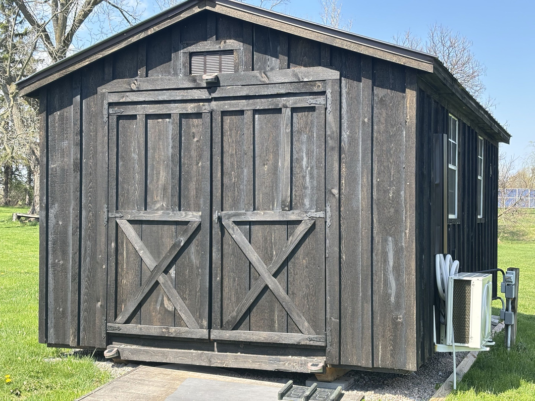
CLEANROOM
The Cleanroom Shed: Bill of Materials
The complete infrastructure BOM for turning a 10×18 ft wooden shed into a working Class 100 cleanroom (walls, air, power, light, and safety) with links for every part.
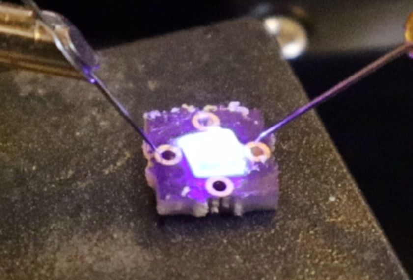
DEVICES
Making LEDs From an Epiwafer
From a commercial InGaN epiwafer to a packaged, glowing LED, laser etching, KOH recovery, bilayer lithography, sputtered contacts, laser dicing, and indium flip-chip packaging. Includes a shortcut version that lights up with a 9V battery.