The hardest part of an LED, the crystal growth, is the part you can buy. A commercial InGaN epiwafer already contains the quantum wells that make the light; everything after that is contacts, geometry, and packaging. This guide covers the full path from a piece of epiwafer to a packaged LED you can solder to, and along the way, a shortcut that gets you to first light with nothing more than a laser, some indium, and a 9V battery.
The epiwafer: what you’re starting with
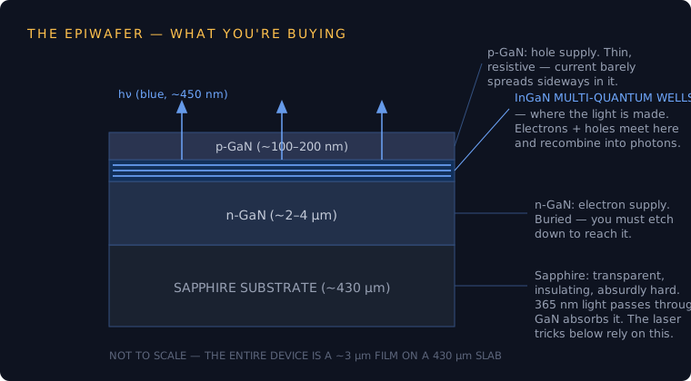
An LED epiwafer is a thin single-crystal film of gallium nitride (GaN) grown on a sapphire disc. Three parts matter:
- n-GaN: a few microns thick, supplies electrons. It’s buried under everything else, so making contact to it means etching down to it.
- The multi-quantum wells (MQW): a stack of nanometer-thin InGaN layers where electrons and holes meet and recombine into blue photons (~450 nm).
- p-GaN: a thin cap that supplies holes. It’s resistive, and current barely spreads sideways in it, which drives several choices below.
For a researcher: standard c-plane LED epi on sapphire, Ga-face up. For everyone else: a mirror-shiny piece of glass-like material that is secretly already 95% of an LED.
Where to buy one
This build used a wafer from PM Optics, which sells red, green, or blue LED epiwafers starting around $160 per 2-inch wafer and a 2-inch wafer diced into millimeter-scale die is a lifetime supply of LEDs for one person. Other suppliers that quote research quantities: UniversityWafer (InGaN MQW LED structures on 2” sapphire, quote-based), PAM-XIAMEN / Powerway (full blue LED structures, ~455 nm), and Ganwafer. One practical note on the China-based suppliers: China has required export licenses for gallium materials since 2023, so lead times can stretch order before you need it.
Tools and materials
| Item | Notes |
|---|---|
| InGaN LED epiwafer piece | see sourcing note above |
| 355 nm laser marking machine | generic “5W 355nm UV Laser Marking Machine, Crystal 3D Inside Carving 2D 3D 2-in-1” unbranded, widely available from China |
| KOH, DI water, hotplate | damage recovery |
| Acetone, IPA, DMSO | cleans and lift-off |
| LOR 5A + AZ1512 + 0.26N TMAH developer | bilayer lithography |
| Spin coater, i-line (365 nm) exposure | see the lithography guide |
| Sputter system | Ni, Ag, Ti targets |
| ENIG-finish PCB, indium bar + sulfamate plating solution | both from Indium Corporation |
| Rosin paste flux, micromanipulator (or improvised press), hotplate to 220 °C | flip-chip bonding |
| Optional: Ce:YAG phosphor powder (25 µm), clear encapsulant | white light conversion |
Safety, before anything else. This process involves a Class 4 UV laser (invisible beam, instant eye damage, proper 355 nm-rated goggles and an enclosed working area are non-negotiable), hot caustic KOH solution, TMAH developer (toxic on skin contact, gloves), hot solvents, and metal fumes from annealing. None of it is exotic by lab standards, and all of it will hurt you if treated casually. Read the SDS for anything you haven’t used before.
Step 1: Laser etching the GaN
The trick that makes this whole guide possible: GaN absorbs 355 nm light, sapphire doesn’t. GaN’s bandgap sits at ~365 nm, so a 355 nm photon is absorbed within the top fraction of a micron and ablates the surface, while the sapphire underneath only responds when the beam is focused hard enough to drive nonlinear absorption. Same laser, two different jobs, selected by focus and fluence.
The machine is a generic 5W 355 nm “crystal engraving” laser marker. No branding, many identical listings online. The knobs that matter, and what they do:
- Frequency (pulse repetition rate): how many pulses per second. Higher frequency spreads the same average power across more pulses, so each pulse is weaker: gentler, shallower, smoother.
- Pulse width: how long each pulse lasts. Shorter pulses concentrate energy in time: higher peak power, more aggressive ablation, more debris.
- Mark speed: how fast the beam scans. Faster means fewer pulses land per spot, so less material removed per pass.
- Number of marks: how many times the pattern repeats. Your depth control: more marks, deeper cut.
For etching the GaN surface: 40 kHz, 4 µs pulse width, 200 mm/s mark speed, a single mark removes roughly 0.5 µm of GaN. That per-mark depth is your calibration stack marks to reach the depth you need. To contact the buried n-GaN you need to get through the p-GaN and MQW (a few hundred nanometers), so a single mark is all it takes to land in the n-layer, that’s what was used here.
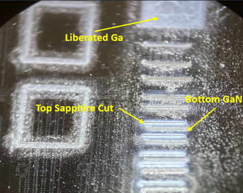
The ablation leaves the surface covered in liberated gallium, metallic Ga droplets freed when the laser decomposes GaN into Ga metal and nitrogen gas. It looks like a dull gray haze over the etched areas. Don’t worry about it; the next step eats it.
Step 2: KOH damage recovery
Laser-etched GaN is not device-quality GaN: the surface is decomposed, Ga-rich, and defective, and contacts made straight onto it behave badly. The fix is cheap: 0.8 wt% KOH in DI water at 80 °C for 1 hour. The hot dilute KOH dissolves the metallic Ga and preferentially attacks the laser-damaged, defective material while barely touching pristine c-plane GaN, so the etch self-limits at a recovered, clean crystal surface.
For newcomers: think of the laser as a chainsaw and the KOH as sandpaper. You need both.
⚡ The easy version: an LED with indium and a 9V battery
Everything past this point is what it takes to make a good LED. But if the goal is a LED, first light, tonight, you can stop the cleanroom work right here:
- Laser-etch trenches down into the n-GaN (Step 1) and optionally do the KOH recovery (Step 2).
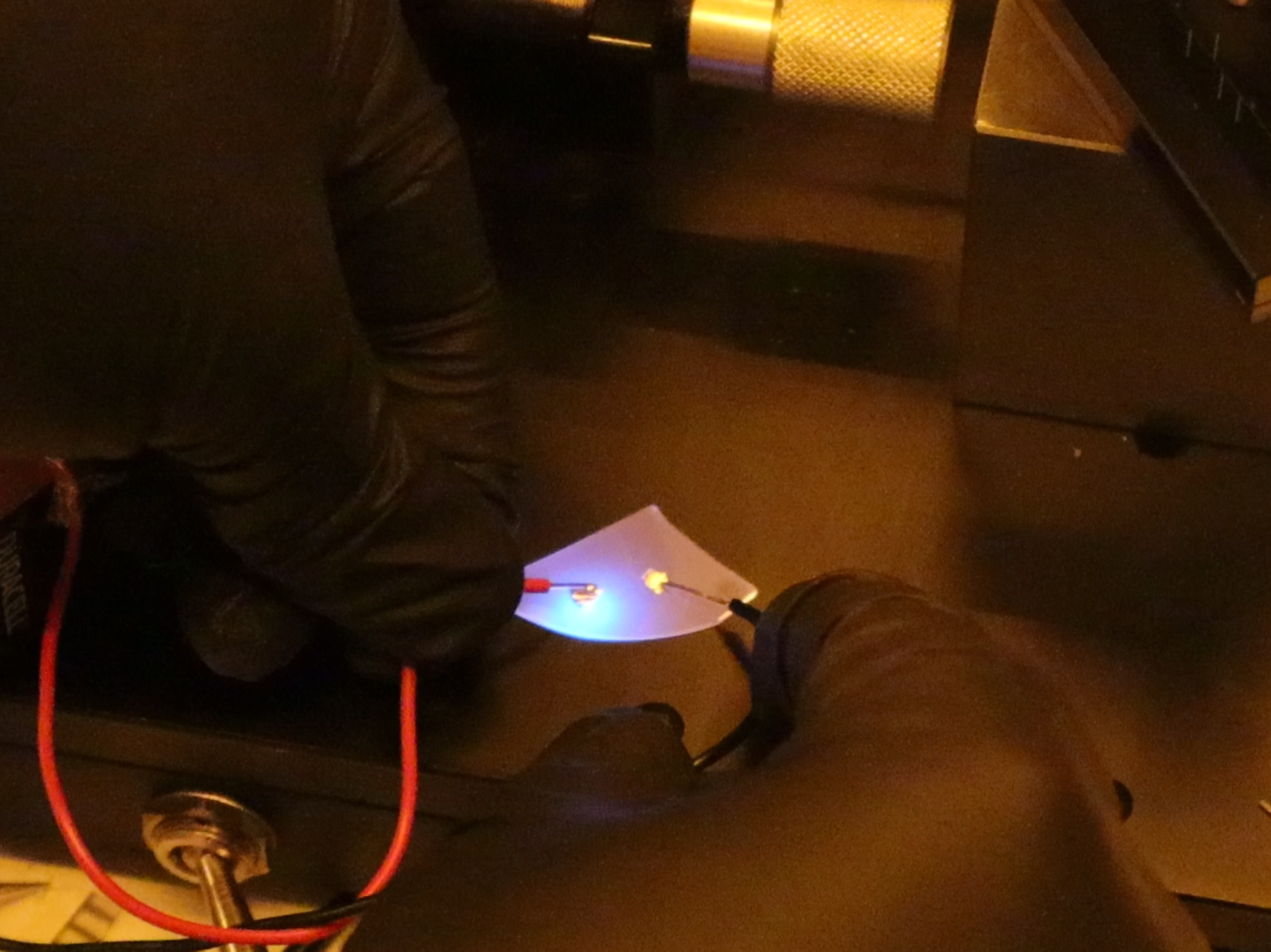
- Press, genuinely just smush, a small piece of indium metal onto the untouched p-GaN top surface, and another into an etched n-GaN trench. Indium is soft enough to cold-weld onto the surface with fingertip or tweezer pressure.
- Touch a 9V battery across the two indium blobs, positive to the p-side. The junction lights up blue.
It won’t be efficient, the indium makes a mediocre contact on p-GaN, and the 9V battery is comically over-voltage for a ~3V diode, put a resistor (a few hundred ohms) in series unless you enjoy living dangerously, since the battery’s internal resistance is doing all the current limiting otherwise. But there is nothing like watching a piece of crystal you processed yourself emit light. This is the demo version; the rest of the guide is the engineering version.
Step 3: Solvent clean
Before lithography, a standard clean: 10 min acetone, 10 min IPA, 10 min DI water, then blow dry. Every fingerprint you leave now is a defect you photograph later.
Step 4: Bilayer lithography
The contacts are patterned by lift-off: pattern resist first, deposit metal over everything, dissolve the resist so metal remains only where the resist wasn’t. For lift-off to work cleanly you need the metal film to break at the pattern edges, which is what the bilayer is for.
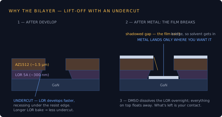
The stack, bottom to top:
| Layer | Spin | Bake | Result |
|---|---|---|---|
| LOR 5A | 2700 rpm, 45 s | 170 °C, 5 min | ~300 nm |
| AZ1512 | 3000 rpm, 30 s | 100 °C, 2 min | ~1.5 µm |
LOR is not photosensitive, it just dissolves quickly in developer, receding under the patterned resist edge to form the undercut. The LOR bake is your undercut control: bake longer for less undercut, shorter for more.
Expose the pattern with ~150 mJ/cm² of i-line (365 nm) light, here, from LEDs through the microscope (see the lithography guide for that system). Develop in 0.26N TMAH for 60 seconds (NaOH or KOH developers also work), rinse in DI water, and blow dry, a filtered hand squeeze pump is enough.
Step 5: The p-contact: Ni/Ag, annealed
Sputter ~30 nm Ni followed by 30 nm Ag, then lift off (Step 6), then anneal in air at ~450 °C for 5 minutes. The air anneal is the point: oxygen converts the nickel into NiO and drives the interface chemistry that makes the contact ohmic on p-GaN, dropping the contact resistivity, and the silver behind it acts as a mirror, bouncing light back out through the sapphire. p-GaN is the hardest material in this process to contact well; this Ni/Ag + air anneal recipe is the workhorse solution.
Step 6: Lift-off
Soak overnight in DMSO with gentle agitation. The DMSO dissolves the LOR, and the metal-on-resist floats away, leaving your contacts. Heating the DMSO speeds this up substantially if you’d rather not wait.
Step 7: Second pattern: the top metal
Repeat the bilayer lithography (identical recipe), this time opening both the n-contact areas (down in the laser-etched, KOH-recovered trenches) and a second layer over the p-contact, so both terminals end up with the same bondable top surface. Sputter 30 nm Ti + 30 nm Ag.
Titanium is the adhesion and n-contact workhorse, but it’s a getter, it grabs any oxygen or water in the chamber and turns into resistive junk mid-deposition. Base pressure below ~10⁻⁶ Torr before you start, and don’t dawdle at low rates. Lift off in DMSO as before.
Step 8: Dicing with the same laser
Now the laser’s second job: cutting the sapphire. This one is all about focus, sapphire only ablates near perfect focus, within about ±0.1 mm, where the intensity is high enough for nonlinear absorption. Out of focus, the cut gets rough or stops happening; the second photo below shows cut lines at different focus depths, with widths running 30–50 µm and roughness growing as focus drifts.
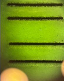
Dicing recipe: 20 kHz, 14 µs pulse width, 150 mm/s, 1,000 marks, stepping the focus 0.1 mm deeper into the material as the cut progresses, chasing the focal point down through the wafer. A useful diagnostic from the first photo in Step 1: cuts made into the top sapphire surface appear white and frosty, while light that passed through the transparent sapphire and was absorbed at the GaN on the far side looks distinctly different, a quick visual check of where your energy is actually landing.
An optional photoresist coat before dicing keeps ablation debris off your finished devices and rinses away afterward.
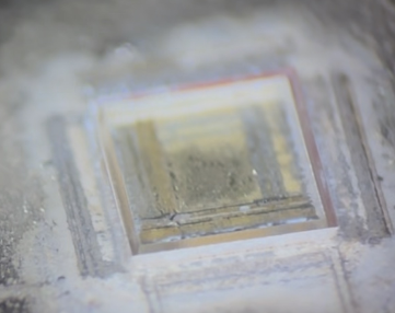
Why dice at the end rather than the start? Because the GaN etch needed the KOH recovery step, and you want all the wet chemistry, spinning, and handling done on one robust piece, not on confetti.
Step 9: Packaging: indium flip-chip
No wire bonder required, the PCB becomes the package. Full details and theory in the packaging guide; the LED-specific version:
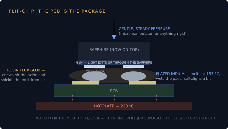
Plate indium onto the board. Take an ENIG-finish PCB (the standard gold finish, order these from any board house), connect wires to the vias, and mask everything except the pads-to-be with Kapton tape. Plate from an indium bar in sulfamate solution (bar and solution both from Indium Corporation) at 400 nA for under a minute, yes, nanoamps: these pads are tiny, and the current scales with how much pad area your design exposes, so treat 400 nA as the setting for this pad density and scale proportionally for yours.
Bond within the hour. Fresh indium grows an oxide skin fast; you want to bond within ~1 hour of plating. A glob of rosin paste flux over the pads protects the indium as it heats and chews off what oxide has formed.
Smush, heat, watch. Place the die face-down, aligning its Ti/Ag pads to the plated pads, a micromanipulator is ideal, but anything that pushes the die down and holds it in contact works. Hotplate underneath to 220 °C (indium melts at 157 °C), and watch: you can see the indium melt and wet. Cool it down, and the LED is bonded, light shining up through the transparent sapphire, connections hidden underneath.
Reinforce. An underfill material adds mechanical strength; honestly, superglue around the die edges works too.
Step 10: Optional: make it white
Blue LED + yellow phosphor = white light, the same trick as virtually every white LED you own. The phosphor is Ce:YAG: yttrium aluminum garnet, a hard transparent crystal, doped with cerium. The cerium absorbs blue light and re-emits it as a broad yellow band; here, 25 µm Ce:YAG powder (peak emission 552 nm), bought from Alibaba. Your eye adds the transmitted blue and the converted yellow together and reads white.
Mix the powder into a clear encapsulant and apply it over the die, since all connections are underneath, you can freely coat the top and edges. This build used Lexel transparent epoxy, air-dried, though a proper silicone like PDMS is the better choice, clearer, more heat-tolerant, and less prone to yellowing over the LED’s life.
Results
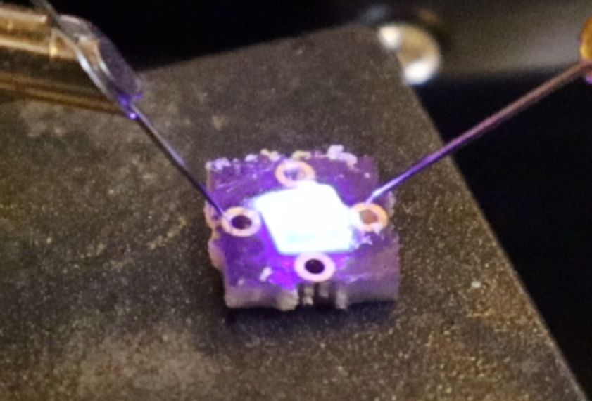
The payoff, the packaged, phosphor-coated LED lit up under probes. The Ce:YAG converts most of the blue to yellow for a white output, with the unconverted blue visible spilling around the die edges.
Related guides: lithography guide (coming soon) and the video version on Dr.Semiconductor.